

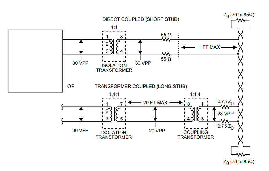
-. 케이블을 통과하는 외부 78ohm 터미네이션
-. plane에 의해 유도된 커패시턴스가 신호에 영향을 미치므로 1553 버스신호는 전원, 접지 plane에서 되도록 멀리 유지한다.
-.1MHz에서 70–85 Ω 임피던스를 갖는다. 원형 커넥터를 사용할 때, 중앙 핀은 하이(high, positive) Manchester bi-phase signal에 사용된다. 전송기와 수신기쌍(Transmitters and receivers couple는 전원장치 차폐 트랜스를 통해 버스에 연결되고, 나머지 연결은 한쌍의 isolation 저항과 하나의 coupling transformer 를 사용
-. BUS A와 BUS B는 배선층을 최대한 이격시킨다.
-. 커플링 변압기를 가능한 1553컨트롤러에 가깝게 배치한다.
GROUND PLANES
As is the rule in all high-speed digital circuits, it is a good practice to use ground and power supply planes under the ACE as well as the host processor and any digital "glue" logic.
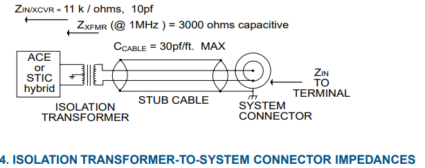
However, it is very important that there be no ground and/or power supply planes underneath the analog bus signal traces. This applies to the TX/RX signals running between the hybrid and the isolation transformer as well as the traces between the transformers to any connectors or cables leaving the board.
The reason for avoiding running supply or ground planes under the analog signal traces is that the effect of the distributed capacitance will be to lower the input impedance of the terminal as seen from the MIL-STD-1553 bus. MIL-STD-1553B requires a minimum of 2k ohm input impedance for direct coupled terminals and 1k ohm for transformer (stub) coupled terminals. If there are ground planes under the analog signal traces, it is likely that the terminal will not meet this requirement. It has been found that placing a ground plane under the isolation transformers only slightly effects the input impedance. A ground and/or power plane may be placed under the transformers, if desired.

POWER AND GROUND DISTRIBUTION
Another important consideration for 1553 transceiver operation is power and ground distribution. Refer to Figure 3.
For the ACE (STIC) hybrid/transformer combination, the high current path when the ACE is transmitting will be from the -15V (or -12V or +5V) power supply, through the ACE's (STIC's) transmitter output stage, through one leg of the isolation transformer to the transformer center tap.
It is important to realize that the high current path is through the transformer center tap and not through the ACE's (STIC's) GNDA and GNDB pins.
Two exceptions to the operation described above are the BU-61590 universal terminal and the BUS-65149 RT hybrid. With these two units, it is important to note that the transmitter provides a differential output stage, actively driving both transformer legs with opposing polarity signals.
For the BU-61590 or BUS-65149, the transformer center tap must not be grounded. In this case, the heavy transmitter supply current runs from the +15/12V (-15/-12V) supply, through the transformer primary and back to the -15/- 12V (+15/-15V) supply. Like the other ACE and STIC units, there will not be a large transmitter return current flowing through GNDA and GNDB.
A worst-case system design should ensure that with minimum supply voltage and calculated voltage drops, the transceiver voltage provided between the ACE's (STIC's) transceiver supply pins and the center tap of the respective isolation transformer will be no less (in absolute value) than the specified minimum (-14.25V, -11.6V, or +4.75V).
In some cases, the voltage drop may be reduced by means of large decoupling capacitors, but the best practice is to minimize voltage drops in the power supply distribution.
ANALOG AND DIGITAL GROUNDS
It is important to note that the logic ground and transceiver grounds are connected together internally in the STIC or ACE hybrids. These grounds must be connected together externally.
As far as the ACE (STIC) and its associated isolation transformer are concerned, the optimal circuit layout would entail a single ground plane for both the digital and analog (transceiver) circuits. While this is sometimes possible, in many applications, there are system requirements for separate analog (-15/-12/+5 (analog)) and digital (+5V) power supply returns.
In this case, the transformer center tap should be connected through a low impedance path to the analog return, not the digital return.
This provides the advantage of separating the analog and digital ground currents. It is assumed that the two return paths are ultimately bonded with low impedance connections to the system ground near the power supply
In order to minimize the possibility of ground noise corrupting the protocol/transceiver interface within the ACE (STIC), it is best that both the LOGIC GND pin as well as the GNDA and GNDB pins be connected to the logic ground as close as possible to the hybrid.
'[기초강의실] > 통신, 규격, DesignGuide' 카테고리의 다른 글
| RS-232(UART), RS-422, RS-432, RS-485 비교 (0) | 2022.05.28 |
|---|---|
| MXM Graphics Module Specification (0) | 2021.06.04 |
| CAN통신개요와 PCB설계기법 (0) | 2019.06.01 |
| I2C 통신개요와 PCB설계기법 (0) | 2019.06.01 |
| Rs422 통신개요와 PCB설계기법 (Rs422 Spec.) (0) | 2019.04.19 |